
Hello (Substack) World
Say 'Hello' to ruthenium. Goodbye copper?

Thanks for taking time out to read the inaugural post of Semi Conscious. This substack can trace its origins back to the first blog of my former employer Semiconductor Insights (now TechInsights). We called that blog SemiSerious. After several engagements writing for EE Times, a regular column there was created under the same banner. I've been doing editorial engagements on and off over the years. EE Times exposed me to a lot of dedicated and knowledgeable readers. I hope to re-engage with those or at least create another community of shared interests.
I will try to mix content of interest to people in the field as well as a wider audience with less technical experience. I will always do the best I can to avoid jargon and keep the topics understandable. If it happens to be too “dumbed down” for you. I hope you will still find something to keep reading.
Writing has never been my day job. That has always been semiconductor analysis through forensics (or reverse engineering, if you prefer) of integrated circuits. RE has been "the gig" since I finished my post doc at the National Research Council of Canada (too ling ago to think about). The purpose of the analysis of the semiconductor products is most often related to the protection of intellectual property. I have been engaged in the assessment of patents for technical merit and market impact throughout my career. It has been a great privilege to have this type of work since it offers a broad perspective on technical developments along with intellectual property and the business side of the industry. I hope to share my knowledge and experience with a wider audience.
About a year and a half ago, I left Ottawa and returned to my roots in Western Canada. I will be writing from the cellar (we say "basement" here in Alberta) of a century farm house, the original from my wife's grandparents’ homestead. That's why you might see occasional references to "dispatches from the cellar."
My writing always needs a little spark of inspiration. For this introductory Semi Conscious, it was Samuel K. Moore’s IEEE Spectrum article on Ru interconnects. An earlier major milestone in interconnects coincided with my early days in mainstream semiconductors / reverse engineering and patents. IBM copper interconnect images abounded. A back to the future moment for me is lightning-level spark.
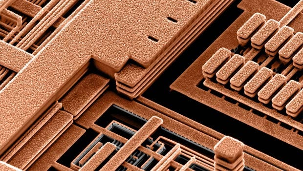
An interesting feature of those IBM copper images was that the lines were all exposed. This led many people to ask what the dielectrics were. Was IBM using air gap technology? No. That was 20th century technology, and the exposed lines were merely a byproduct of sample preparation to make the interconnect metals visible to a SEM beam. For electron beam imaging to work and the lines not to be obscured by the silicon dioxide dielectric stacks, the material had to be removed. The use of air gaps would come later.
Keep reading with a 7-day free trial
Subscribe to Don Scansen, Semi Conscious to keep reading this post and get 7 days of free access to the full post archives.